Mitä suureita olet mitannut?En ole ymmärtänyt, en ymmärrä mihin tuota akkulaturia.....no varaajaa kylläkin ladataan mutta ihan eri juttu kun 12v akun lataaminen.
Olen testaillut kuudella (6) 8*270W sarjaankytketyllä ryhmällä.
En jaksa vääntää, puhutaan ihan eri asioista.

Navigaatio
Asenna sovellus
Sovelluksen asentaminen iOS:ssä
Seuraa alla olevaa videota nähdäksesi, miten asennat sivustomme verkkosovelluksena aloitusnäytöllesi.
Huom.: This feature may not be available in some browsers.
Lisää vaihtoehtoja
Teeman tyyli
Käytät vanhentunutta selainta. Selaimesi ei mahdollisesti näytä tätä tai muita sivustoja oikein. Sinun tulisi päivittää selaimesi tai käyttää vaihtoehtoista selainta..
Aurinkosähköjärjestelmän komponenteista höpinää
- Viestiketjun aloittaja fraatti
- Aloituspäivämäärä
Niin mistähän sinä puhut eli mitä olet testannut?En ole ymmärtänyt, en ymmärrä mihin tuota akkulaturia.....no varaajaa kylläkin ladataan mutta ihan eri juttu kun 12v akun lataaminen.
Olen testaillut kuudella (6) 8*270W sarjaankytketyllä ryhmällä.
En jaksa vääntää, puhutaan ihan eri asioista.
Tuossa on oleellista käyttää säätäjää, jossa on hakkurimuunnin, joka kasvattaa virtaa jännitteen laskiessa, jolloin hyötysuhde pysyy reilusti yli 90% paneelista saatavasta tehosta riippumatta. Akkulataukseen suunnitellut MPPT-säätimet toimivat noin. Niitä saa eri tehoille ja jännitteille. En tiedä millaisista tehoista @Mikki on kiinnostunut. IV-kanaviin ei voi yleensä laittaa kuin 1-2 kW.
Lueskelin huvikseen tuollaista "Photovoltaic Roadmap (ITRPV): Eleventh Edition(April 28, 2020)" läpyskää ja siinä valotetaan vähän mitä mitä kehitys tuo tullessaan.
-2020 monokidekiekkoja 75% ja 2030 enää vain 5% monikidekennoja
-piikiekon koko tulee kasvamaan 56.75 x 156.75 mm² → 166.0 x 166.0 mm² → 210.0 x 210.0 mm² (?)
-perc ja half cutti yleistyy entisestään
-tehot ilmoitetaan Wp/m2 kun panelien koot tulevat muuttumaan
-nyt keskiteho PERCissä noin 320 Wp ja 2030 360 Wp (62 kennoinen paneli nykyisissä mitoissa)
Hintakehitys:

-2020 monokidekiekkoja 75% ja 2030 enää vain 5% monikidekennoja
-piikiekon koko tulee kasvamaan 56.75 x 156.75 mm² → 166.0 x 166.0 mm² → 210.0 x 210.0 mm² (?)
-perc ja half cutti yleistyy entisestään
-tehot ilmoitetaan Wp/m2 kun panelien koot tulevat muuttumaan
-nyt keskiteho PERCissä noin 320 Wp ja 2030 360 Wp (62 kennoinen paneli nykyisissä mitoissa)
Hintakehitys:
The market share of monocrystalline silicon (mono-Si) wafers in 2020 will be close to 75 percent and will continue to grow. In contrast, the market share of multicrystalline silicon (mc-Si) wafers will shrink continuously from about 20 percent in 2020 down to only 5 percent until 2030. The 2019 dominating wafer format of 156.75 x 156.75 mm² will disappear within the next 3 years and will be replaced fast by larger formats. Future mainstream will be formats of 166.0 x 166.0 mm² (M6) or even larger ones like 210.0 x 210.0 mm² (M12).
The continued roll out of PERC cell technology and the implementation of half-cell module technology enabled higher performing module products in 2019. Due to the current diversification in wafer formats, module dimensions are also changing. The comparison of different module types only by the common module label power may be misleading as module powers of ≥ 500 Wp are possible today with existing cell technologies by using larger wafer formats. Module area efficiency (module label power divided by module area in m²) is therefore a helpful parameter to compare different module types and module technologies.
PERC p-type mono-Si modules show an average area efficiency of 203 W/m² in 2020. This will increase to 225 W/m² in 2030. Modules with n-type cell concepts, especially those using tunnel oxide passivation technologies, are expected to be ahead of p-type PERC with 208 W/m² in 2020 and with up to 230 W/m² until 2030. HJT modules reach area efficiencies of 210 W/m² in 2020 and are expected to outperform other c-Si module types with close to 240 W/m² within the next 10 years.
Viimeksi muokattu:
Tuossa on oleellista käyttää säätäjää, jossa on hakkurimuunnin, joka kasvattaa virtaa jännitteen laskiessa, jolloin hyötysuhde pysyy reilusti yli 90% paneelista saatavasta tehosta riippumatta. Akkulataukseen suunnitellut MPPT-säätimet toimivat noin.
Ainakin lyijyakkulaturi on tyypillisesti sellainen että se haluaa nähdä suunnilleen tasajännitekuorman, ja työntää siihen sitten sen verran virtaa kuin akku ottaa, tai kuinka paljon on annettavaa (kumpi raja nyt tulee ensin vastaan).
Jos vastuksen pistää kuormaksi tollaiseen ni eri tuottotehoilla se "akun napa"-jännite muuttuu tehon suhteessa eikä laturi välttämättä osaa työntää sähköä väärään jännitteeseen.
MPPT latureista ei ole niin paljoa kokemusta että tietäisin toimivatko nuin...
-Topi

pökö
Kaivo jäässä
Ei se nyt niin ihmeitä nouse, aika rauhallisia nousut on.VILP tapauksessa COP kuitenkin nousee aika kohinalla lämpötilan noustessa.
Hintakehitys:
Toi experience learning curve on jännä keksintö. Vaaka-akselilla on kumulatiivinen tuotanto, ja pystyakselilla näkyy tuotannon kokemuksesta ja kysynnän kasvamisesta saatava etu (hinnanalennus).
Kun se piirretään log-log asteikolle ni yllättävän usealla tuotteella siihen syntyy noin suora. Eri tuotteilla toki eri kulmakertoimella.
Fraattin kuvassa on historiadataa 70-luvun puolestavälistä tähän päivään, ja varsinkin alussa näyttää pysyneen tolla suoralla.
Jossain muistan nähneeni todistuksen että uudismarkkinoiden valtaustilanteessa (ei-suojatut markkinat), jos toi experience learning pätee, on taloudellisesti järkevää myydä tuotteita niin halvalla kuin takapuoli vain kestää, jotta saa volyymiä ylös ja sitäkautta kokemuksella saatavaa hintaetua. Se joka ei näin tee, ei voi pärjätä kilpailussa, kun omakustannushinta jää eksponentiaalisesti jälkeen kilpailijoiden hinnasta.
-Topi
MPPT-laturi on yleensä buck-muunnin, jonka virtaa rajoitetaan niin, että tulojännite pysyy optimaalisena. Lähtöjännite sitten on mikä on, kunnes se on niin korkea, että sen takia rajoitetaan virtaa. Noille määritetään maksimivirta joka tulee lähinnä kelasta. Se rajoittaa lähtöjännitettä.MPPT latureista ei ole niin paljoa kokemusta että tietäisin toimivatko nuin...
Tuollaisen olen omaan veneeseeni suunnitellut ja rakentanut.
MPPT-laturi on yleensä buck-muunnin, jonka virtaa rajoitetaan niin, että tulojännite pysyy optimaalisena. Lähtöjännite sitten on mikä on, kunnes se on niin korkea, että sen takia rajoitetaan virtaa. Noille määritetään maksimivirta joka tulee lähinnä kelasta. Se rajoittaa lähtöjännitettä.
Tuollaisen olen omaan veneeseeni suunnitellut ja rakentanut.
Juu, noita hakkureita on kanssa tullut työnkin puolesta suunniteluta erilaisia.
Tarkoitin lähinnä sitä, että 12 voltin lyijyakun lataukseen tarkoitettu laite ei (mun mielestä) toimi oikein jos se 9 voltin kuormaan suostuu ajamaan virtaa. Tai 16 voltin.
-Topi
Toi experience learning curve on jännä keksintö. Vaaka-akselilla on kumulatiivinen tuotanto, ja pystyakselilla näkyy tuotannon kokemuksesta ja kysynnän kasvamisesta saatava etu (hinnanalennus).
Kun se piirretään log-log asteikolle ni yllättävän usealla tuotteella siihen syntyy noin suora. Eri tuotteilla toki eri kulmakertoimella.
Fraattin kuvassa on historiadataa 70-luvun puolestavälistä tähän päivään, ja varsinkin alussa näyttää pysyneen tolla suoralla.
Jossain muistan nähneeni todistuksen että uudismarkkinoiden valtaustilanteessa (ei-suojatut markkinat), jos toi experience learning pätee, on taloudellisesti järkevää myydä tuotteita niin halvalla kuin takapuoli vain kestää, jotta saa volyymiä ylös ja sitäkautta kokemuksella saatavaa hintaetua. Se joka ei näin tee, ei voi pärjätä kilpailussa, kun omakustannushinta jää eksponentiaalisesti jälkeen kilpailijoiden hinnasta.
-Topi
Tuossa yksi syy, kennot ohentuneet ja hukka vähentynyt.

16 V ei anna. Antaa enintään 14,8 V ja senkin yleensä vain tietyn ajan, jonka jälkeen tiputtaa ylläpidolle (esim. 13,6 V). Tuollaiseen pitäsi siis paneeli vs. vastus mitoittaa niin, ettei tuo 13,6 V ylity koskaan. Joissain akkulatureissa on tosiaan suojaussysteemi, jolla estetään alijännitteisen akun lataus. Eli saattaa olla, että jotkut eivät toimi esim. alle 10 V. Mutta silloin kyse on tosiaan akun suojelun takia tehdystä estosta.Tarkoitin lähinnä sitä, että 12 voltin lyijyakun lataukseen tarkoitettu laite ei (mun mielestä) toimi oikein jos se 9 voltin kuormaan suostuu ajamaan virtaa. Tai 16 voltin.
Aika monessa laitteessa on automaattivalinta 24 vs.12 V. Tiedä sitten miten tuo valinnan tekee, mutta periaattessa tuon on toimittava 10-27 V.
16 V ei anna. Antaa enintään 14,8 V ja senkin yleensä vain tietyn ajan, jonka jälkeen tiputtaa ylläpidolle (esim. 13,6 V). Tuollaiseen pitäsi siis paneeli vs. vastus mitoittaa niin, ettei tuo 13,6 V ylity koskaan. Joissain akkulatureissa on tosiaan suojaussysteemi, jolla estetään alijännitteisen akun lataus. Eli saattaa olla, että jotkut eivät toimi esim. alle 10 V. Mutta silloin kyse on tosiaan akun suojelun takia tehdystä estosta.
Aika monessa laitteessa on automaattivalinta 24 vs.12 V. Tiedä sitten miten tuo valinnan tekee, mutta periaattessa tuon on toimittava 10-27 V.
Meillä on suurena aarteena muuntajalla ja sillalla tehty tarpeeksi brutaali akkulaturi jolla saa liian tyhjäksi päässeen akun taas ladattua. On siinäkin jo joku kytkentä joka huomaa akun täyttyvän, mutta se ei kaipaa jännitettä akun päästä lähteäkseen käyntiin. Kesäisin se on antamassa sähköä kasvihuoneen kastelupumpulle.
Aurinkopanelien hinta alkaa olla jo samaa suuruusluokkaa kuin katon pintamateriaalien. Saako vesikaton jotenkin tehtyä paneeleista? Tuntuu hölmöltä laittaa paneelien alle vesikatto ja telineet, jos olisi mahdollista yhdistää ne.
Millainen on ollut invertterien hintakehitys? Halpeneeko nekin samaa vauhtia? Entä kiinnikkeet? Luulenko vain, että paneelit ovat pian halvin osa systeemistä?
Millainen on ollut invertterien hintakehitys? Halpeneeko nekin samaa vauhtia? Entä kiinnikkeet? Luulenko vain, että paneelit ovat pian halvin osa systeemistä?
Viimeksi muokattu:
K
korsteeni
Vieras
Varmasti onnistuu ihan sica massalla panelit yhteen, on pitävämpi kuin muut materiaalit, mutta, mutta, kuka uskaltaa ilman tiiltä/peltiä laittaa kuitenkin paloriskin omaavat laitteet lautaruotuihin katolle, minä en ainakaan, eri juttu erillisissä telineissä tai vaikkapa autokatoksen päällä, autot halpoja eikä joudu itse ulkosalle käryn käydessä.Aurinkopanelien hinta alkaa olla jo samaa suuruusluokkaa kuin katon pintamateriaalien. Saako vesikaton jotenkin tehtyä paneeleista? Tuntuu hölmöltä laittaa paneelien alle vesikatto ja telineet, jos olisi mahdollista yhdistää ne.
Millainen on ollut invertterien hintakehitys. Halpeneeko nekin samaa vauhtia? Entä kiinnikkeet? Luulenko vain, että paneelit ovat pian halvin osa systeemistä?
Ohan niitä aurinkotiilikattoja ja ties mitä jo kehitelty. Mutta en usko, että pelkkä aurinkopaneeli vesikattona menisi rakennusvalvonnalta läpi. Eiköhän sieltä löydy joki direktiivi tai standardi mikä estää. Toisekseen mitä sitten kun yksi paneeli rikkoutuu ja sitä ei ole enää saatavilla? Tai jos joutuu kulkemaan katolla?Aurinkopanelien hinta alkaa olla jo samaa suuruusluokkaa kuin katon pintamateriaalien. Saako vesikaton jotenkin tehtyä paneeleista? Tuntuu hölmöltä laittaa paneelien alle vesikatto ja telineet, jos olisi mahdollista yhdistää ne.
Millainen on ollut invertterien hintakehitys? Halpeneeko nekin samaa vauhtia? Entä kiinnikkeet? Luulenko vain, että paneelit ovat pian halvin osa systeemistä?
Millainen on ollut invertterien hintakehitys? Halpeneeko nekin samaa vauhtia? Entä kiinnikkeet? Luulenko vain, että paneelit ovat pian halvin osa systeemistä?
Tässä on mainittu että järjestelmien kokonaishinnat olisi tulleet alaspäin 13% vuosivauhtia. Itse paneleiden osuus kokonaishinnasta alle puolet.

Aurinkosähkö vs muut tuotantomuodot

Itse inverttereistä

Painoa on ainakin lähtenyt reilusti pois vuosien saatossa

Hintakehityksestä

Ohan niitä aurinkotiilikattoja ja ties mitä jo kehitelty. Mutta en usko, että pelkkä aurinkopaneeli vesikattona menisi rakennusvalvonnalta läpi. Eiköhän sieltä löydy joki direktiivi tai standardi mikä estää. Toisekseen mitä sitten kun yksi paneeli rikkoutuu ja sitä ei ole enää saatavilla? Tai jos joutuu kulkemaan katolla?
Miten muuten vikaantuneen paneelin paikallistaa, jos lappeella on 30 paneelia? Ja toisekseen... miten yhden invertterin kanssa käy paneeliston tuotolle, jos yksi vikaantuu?
Yhdelle puolitutulle käni niin, että yksi paneeli pimeni, mutta sillä oli mikroinvertterit joissa kaksi paneelia kiinni, niin piti tarkistaa vain kaksi paneelia että vikaantuneen löysi.
Aika monessa paneelissa on diodit, joiden pitäisi ohittaa ko. paneeli. Samahan tapahtuu jos yksi paneeli on varjossa.Miten muuten vikaantuneen paneelin paikallistaa, jos lappeella on 30 paneelia? Ja toisekseen... miten yhden invertterin kanssa käy paneeliston tuotolle, jos yksi vikaantuu?
Yhdelle puolitutulle käni niin, että yksi paneeli pimeni, mutta sillä oli mikroinvertterit joissa kaksi paneelia kiinni, niin piti tarkistaa vain kaksi paneelia että vikaantuneen löysi.
Tuollainen iso järjestelmä kannattaa tehdä useammalla invertterillä. Ja sellaisella invertterillä missä on monta mppt träkkeriä. Eli jos yksi lenkki alkaa piiputtaa, niin sen 30 paneelin sijasta pitää tarkistaa vain 10 paneelia. Ts. 1 rivi. Mikroilla tuollaista isoa kenttää tuskin kannattaa rakentaa. Alkaa mikroille ja kaapeloinnille tulla hintaa.
Eikö panelit ole standardikokoisia eli ei tarvitse olla samanlainen? Eikö panelit kestä kävelyä? Ainakin ne saa kestämään kävelyä. Veneeni katolla on hiukan taipuisa teräslevyn päälle tehty paneeli, jonka päällä voi kävellä. Siis 3 mm paksu koko roska. Voisihan sellainen olla hyvin koko kone/lukkosaumakaton peltiin yhdistetty. Nuo ovat olleet todella paljon kalliimpia kuin kiinteät tyypillisesti katolle asennettavat, mutta hinnat ovat tippuneet noissa vielä rajummin. Maksoin 2013 50 W tuollaisesta n. 100 €. Tuolloin oli paljon 300 € 50 W paneeleita myynnissä. Nyt saa reilulla satasella jo 200 W.Ohan niitä aurinkotiilikattoja ja ties mitä jo kehitelty. Mutta en usko, että pelkkä aurinkopaneeli vesikattona menisi rakennusvalvonnalta läpi. Eiköhän sieltä löydy joki direktiivi tai standardi mikä estää. Toisekseen mitä sitten kun yksi paneeli rikkoutuu ja sitä ei ole enää saatavilla? Tai jos joutuu kulkemaan katolla?
Noista kovista paneeleista lienee helppo kehittää malli, joka soveltuu kattomateriaaliksi. Onhan niissä jo metallirunko. Lasipinta ehkä pitää vaihtaa laminaattiin ja kehittää systeemi, jolla nuo saa vesitiiviiksi kokonaisuudeksi ja rikkinäiset voi vaihtaa.
Luulisi nykyaikana olevan intoa saada ainakin uudiskohteisiin koko katon kokoiset paneelit suoraan kattoon.
Miten muuten vikaantuneen paneelin paikallistaa, jos lappeella on 30 paneelia? Ja toisekseen... miten yhden invertterin kanssa käy paneeliston tuotolle, jos yksi vikaantuu?
Esim lämpökameralla. ->
Lämpökamerakuvausten hyödyntäminen aurinkovoimalan kunnontarkastelussa

Tai yksittäisten paneleiden tyhjäkäyntijänniteitä voi myös verrata toisiinsa. Samoin oikosulkuvirtoja.
Se mitä tuotolle tapahtuu taitaa riippua vauriosta. Todennäköisyys taas panelin laadusta.

Näyttää hintakehitys pahasti hyytyneen 2012 jälkeen. Kuudessa vuodessa 1400->1100 € eli n. 4% vuodessa. Paneelien osuus tuossa ajassa tippunut 52->45% eli niiden hinta 728->495 eli 6% vuodessa. Loppuosa 672->605 eli 2% vuodessa.Tässä on mainittu että järjestelmien kokonaishinnat olisi tulleet alaspäin 13% vuosivauhtia. Itse paneleiden osuus kokonaishinnasta alle puolet.
Eikö nuo kovat panelit voisi vaan laittaa hiukan päällekkäin tiilikaton tapaan? Siis lisätä runkoon lipat, jolloin nuo katolle ladottaessa muodostaisi tiilikattomaisen rakenteen. Eihän tiili- tai profiilipeltikattokaan vesitiivis ole, vaan kerää vain ehkä 99% vedestä pois aluskatteelta.
Eikö panelit ole standardikokoisia eli ei tarvitse olla samanlainen? Eikö panelit kestä kävelyä?
Perinteiset 60 tai 72 kennoiset paneleiden ulkomitat vaihtelevat valmistajan mukaan. Ei ole mitään standardikokoa. Toki parin sentin tarkkuudella se on 60 kennoisessa tällähetkellä 1 x 1,6m (ellei ole half-cutti).
Panelien kennot ottavat itseensä vaikkei silmiinnähtäviä vaurioita tulisikaan. Niihin tulee mikrohalkeamia.
What are micro cracks?
What are micro cracks? <p><img src="/uploads/media_images/30264dffa4e58a62c4a01da3453f4bfe8b402993.jpeg" style="float: left; margin: 0px 10px 10px 0px; display: block; text-align: left; width: 324.881px; height: 206px;" alt="solar panel micro cracks"></p> <p>Silicon solar cells are made of very...
Eikö nuo kovat panelit voisi vaan laittaa hiukan päällekkäin tiilikaton tapaan? Siis lisätä runkoon lipat, jolloin nuo katolle ladottaessa muodostaisi tiilikattomaisen rakenteen. Eihän tiili- tai profiilipeltikattokaan vesitiivis ole, vaan kerää vain ehkä 99% vedestä pois aluskatteelta.
Katoiksi tarkoitettuja paneleita on erikseen. Esim täällä
Aurinkoenergia -Kattotiilituotteet | Figmentor Oy
 aurinkosahkoa.com
Lisäksi on näitä, mm virtesolar

Perinteiset 60 tai 72 kennoiset paneleiden ulkomitat vaihtelevat valmistajan mukaan. Ei ole mitään standardikokoa. Toki parin sentin tarkkuudella se on 60 kennoisessa tällähetkellä 1 x 1,6m (ellei ole half-cutti).
Panelien kennot ottavat itseensä vaikkei silmiinnähtäviä vaurioita tulisikaan. Niihin tulee mikrohalkeamia.
What are micro cracks?
What are micro cracks? <p><img src="/uploads/media_images/30264dffa4e58a62c4a01da3453f4bfe8b402993.jpeg" style="float: left; margin: 0px 10px 10px 0px; display: block; text-align: left; width: 324.881px; height: 206px;" alt="solar panel micro cracks"></p> <p>Silicon solar cells are made of very...www.lgenergy.com.au
Tilasin pari vuotta sitten Kiinasta paketillisen noita raaka-kennoja. Ihan saadakseni tuntuman miltä ne näyttää ja tuntuu.
Ovat erittäin herkkiä hajoamaan. Paksuutta muutama kymmenesosamilli, ja taivutusta ei tartte kennon päästä montaa milliä kun naksahtaa kappaleiksi. Samalla geometrialla oleva lasi olisi huomattavasti joustavampaa (mutu-väite).
-Topi
virtuaaliharri
Aktiivinen jäsen
Noi suoraan vesikatoksi tarkoitetut aurinkopaneelit taitavat yleensä olla ohutkalvotekniikkaa, jonka ennustettiin (tai on väitetty jo olleen) edullisempaa tekniikkaa kuin perinteiset piipohjaisiin kennoihin pohjautuvat paneelit. Piikennojen halpeneminen on tainnut torpedoida aika tehokkaasti noiden varsinaisten kattotuotteiden markkinat, mutta kyllä noita uusia yrittäjiä kuitenkin näyttää pikkuhiljaa ilmaantuvan: äsken googlatessani tuli vastaan Kerabit aurinkokatto, jota en muista aiemmin nähneeni (mikä ei tarkoita ettenkö varmasti ole nähnyt, sillä on tuo näköjään ollut markkinoilla jo jokusen vuoden).
Kaiketi noille tavallisille paneeleille voisi kehittää teräksisen kattoristikkorakenteen ruoteineen ja paneelien välit tiivistää jonkinlaisella elastisella nauhalla, jonka voi irroittaa paneeleita vaihdettaessa. Samalla pääsisi eroon homehtuvasta materiaalista yläpohjassa. Varmemman vakuudeksi voisi paneelien alapuolella kulkea saumojen kohdalla kourut ohjaamassa mahdolliset vuotovedet kastelemasta alapuolisia rakenteita.
Kaiketi noille tavallisille paneeleille voisi kehittää teräksisen kattoristikkorakenteen ruoteineen ja paneelien välit tiivistää jonkinlaisella elastisella nauhalla, jonka voi irroittaa paneeleita vaihdettaessa. Samalla pääsisi eroon homehtuvasta materiaalista yläpohjassa. Varmemman vakuudeksi voisi paneelien alapuolella kulkea saumojen kohdalla kourut ohjaamassa mahdolliset vuotovedet kastelemasta alapuolisia rakenteita.
Riippuu järjestelmästä. Jos kyse on 12 V järjestelmästä ja 12 V akuista, rinnan voi laittaa ihan kuinka monta akkua huvittaa eikä tarvitse edes olla kapasiteetiltaan samoja.Voiko akkuja laittaa parittoman määrän järjestelmään. Löytyy 3kpl 150ah akkuja.
Sarjankytkentä on sitten huomattavasti vaativampi tapaus.

Kellarinlämmittäjä
Oppimiskäyrällä
On se rinnan kytkeminekin. Pitäisi olla niiden akkujen samassa elinkaaren vaiheessa. Yksi vanha uusien kanssa rinnan purkaa ne uudet jos jäävät seisomaan. Jos akut ovat eri merkkiä ja ikään kuin vähän eri tyyppiä (vaikka nyt olisivatkin 12 V lyijyakkuja), niissä on myös eroja jännitteen kestoissa ja taipuksessa kehittää vetyä. Asialla voi olla merkitystä, kun niitä ladataan. Yksi tykkää ottaa virtaa sisäänsä ja kaveri vieressä kuplii iloisesti.
K
korsteeni
Vieras
Kyllä jmaja on oikeilla jäljillä, se kupliva yksilökään ei haittaa siellä seassa koska se vaatii kupliakseen korkeamman jännitteen eikä sitä synny terveiden akkujen pitäessä jännitteet kurissa, säätimen toimiessa, rinnan ok mutta sarjassa, ne on hyvä olla jopa samaa sarjaaOn se rinnan kytkeminekin. Pitäisi olla niiden akkujen samassa elinkaaren vaiheessa. Yksi vanha uusien kanssa rinnan purkaa ne uudet jos jäävät seisomaan. Jos akut ovat eri merkkiä ja ikään kuin vähän eri tyyppiä (vaikka nyt olisivatkin 12 V lyijyakkuja), niissä on myös eroja jännitteen kestoissa ja taipuksessa kehittää vetyä. Asialla voi olla merkitystä, kun niitä ladataan. Yksi tykkää ottaa virtaa sisäänsä ja kaveri vieressä kuplii iloisesti.
Tietysti jos tietää että akku on paska , ei sitä kannata enää käyttää rinnankaan
Minulla on jus nyt 2*100Ah + 1* 115Ah + 1* 60Ah + 2* pikkuakkua 7Ah (moottoripyörä/jetti) + 1* 9Ah rinnan, pysyvät hyvin pirteänä eikä tarvitse huolehtia sen kummempia
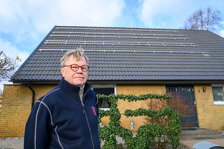
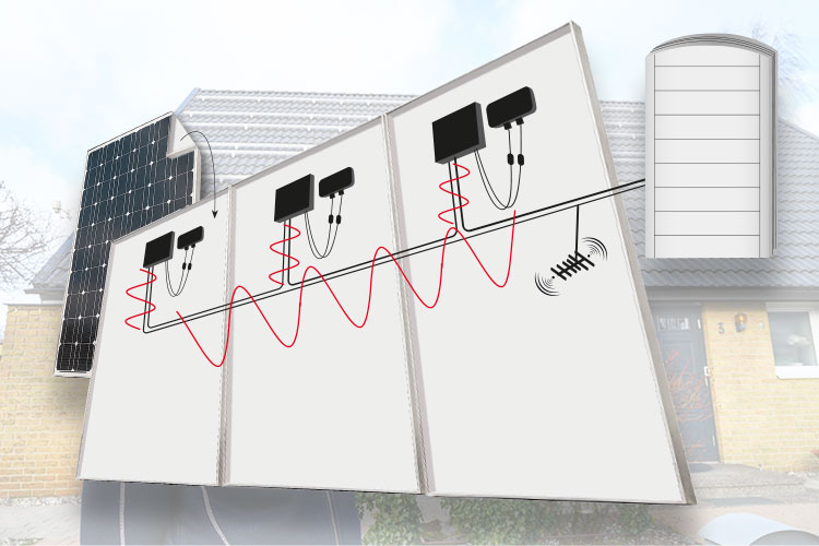
Ruotsissa oli jouduttu solaredgen optimoijilla varustettu aurinkovoimala nyppäämään pois katolta puolustusvoimille aiheutuneiden häiriöiden takia. Häiriö on tullut kaapeloinneista paneelien/optimoijen/invertterin välillä.
"The radio interference is mainly due to the antenna loop that is formed during installation between the solar panels, optimizers / micron inverters and / or inverters."
 www.elinstallatoren.se
"The radio interference is mainly due to the antenna loop that is formed during installation between the solar panels, optimizers / micron inverters and / or inverters."
Per-Ove tvingades ta ner solcellerna: ”De stör”
Mobiloperatörer, Försvarsmakten, Luftfartsverket och radioamatörer – allt fler klagar på störande solceller. Vi har träffat Per-Ove Jönsson som fick plocka ner sina paneler.
www.elinstallatoren.se
Viimeksi muokattu:
Pämpölumppu
Jäsen
Häiriöiden vähentämiseksi suositellaan tässä jutussa että dc+ ja dc- kaapeleista tehdään kierretty pari...
Kierretty pari säteilee varmasti vähemmän mutta saattaa ehkä olla hankala toteuttaa käytännössä invertterille asti?
 www.elinstallatoren.se
Kierretty pari säteilee varmasti vähemmän mutta saattaa ehkä olla hankala toteuttaa käytännössä invertterille asti?
Därför stör solcellerna
Elsäkerhetsverket fick i fjol in tio anmälningar om störande solcellsanläggningar. Alla har en gemensam nämnare.
www.elinstallatoren.se
Harrastelija
Hyperaktiivi
Eikös se paneelien ja invertterin välin saa helpostikin kierrettynä? Onko ongelma enemmänkin paneelien välisissä vedoissa kun ei ole paria mitä kytkeä vaan yksi piuha pelkästään? Tai noh riippuu miten paneelit kytkee.Kierretty pari säteilee varmasti vähemmän mutta saattaa ehkä olla hankala toteuttaa käytännössä invertterille asti?
Onko MCMK kaapelissa piuha kierrettyä? AMKA kaapelissa on.

Voimavirtakaapelia saa myös EMC suojattuna mutta en tiedä onko kierrettyä. Ja taitaa olla 4x eli ylimääräisiä piuhoja jolloin suojaus saattaa kärsiä kun ei ole ”symmetrinen” kuormitus. Ehkä toimii jos käyttää vastakkaisia piuhoja ja välipiuhat maihin.
DC jännitekesto on kylläkin syytä varmistaa vaikka onkin voimakaapelia.
Eivät kylläkään halpoja vaihtoehtoja.
Viimeksi muokattu:

Espejot
Hyperaktiivi
Onko kellään tietoa/kokemusta tämän firman tuotteista?

Itseäni vapaa sijoitelu miellyttää... saisi lisää tunteja kohtuu edullisesti. Myykö kukaan muu mikroinverteripaketteja paneeleineen?
Onko noi Enphase iQ7 microinverterit hyväksyttyjä Suomessa... pitkä takuu niillä ainakin on.
Products and Services - Microinverters (DE-DE)
Enphase Energy: Intelligente Solartechnologie und saubere Energie für jedermann
Saksan säädöillä saa ajella Suomessa.
Espejot
Hyperaktiivi
Products and Services - Microinverters (DE-DE)
Enphase Energy: Intelligente Solartechnologie und saubere Energie für jedermannenphase.com
Saksan säädöillä saa ajella Suomessa.
Katselin että Saksassa aika huono saatavuus... sitten vilkaisin asennustiheyttä. Mars Hollantiin tai Ranskaan...
Epäilyttääkö tämä firma vai miksi haet vastaavaaItseäni vapaa sijoitelu miellyttää... saisi lisää tunteja kohtuu edullisesti. Myykö kukaan muu mikroinverteripaketteja paneeleineen?
Espejot
Hyperaktiivi
Epäilyttääkö tämä firma vai miksi haet vastaavaa
Ei oikeastaan.... toki firma on nuori ja takuut kait hoituu mutakin kautta. Mutta loppupeleissä taidan tutkia asiaa lisää ja itseni tuntien valitsen jonkun länsimaisen firman tuotteita. Mutta taputellaan tää korona ensin.
pökö
Kaivo jäässä
Miksi joku firma, miksei omat kädet ja tekemisen meininki? Sähkäri sitten erikseen.Ei oikeastaan.... toki firma on nuori ja takuut kait hoituu mutakin kautta. Mutta loppupeleissä taidan tutkia asiaa lisää ja itseni tuntien valitsen jonkun länsimaisen firman tuotteita. Mutta taputellaan tää
Espejot
Hyperaktiivi
Miksi joku firma, miksei omat kädet ja tekemisen meininki? Sähkäri sitten erikseen.
Kunhan katselen että mitä myydään... itse ajatelin asentaa ja todenäköisesti komponentit valita. Mutta lusitaan ensin tää kesä.